
What Is Graphene? The Wonder Material Made With Sticky Tape
Every time you write with a pencil, you smear thin flakes of graphite across the page, and a few of them may be just one atom thick. That single layer is the answer to what is graphene: a flat sheet of carbon atoms linked in a honeycomb pattern, so thin it is effectively two-dimensional. It was hiding in pencil lead the whole time. In 2004, two physicists in Manchester found a way to pull it out with sticky tape, and six years later that won them a Nobel Prize.
The story has three parts. There is the trick that isolated graphene, the physics that makes it so strange, and the long, bumpy road from lab flakes to products. The last part is where the hype and the reality have parted ways.
A material physics said shouldn’t exist
Graphite, the grey stuff in pencils, is a stack of carbon layers. According to the Royal Swedish Academy of Sciences’ popular summary of the 2010 Nobel Prize in Physics, one millimeter of graphite holds about three million layers. The layers are weakly held to each other, which is why graphite slides off onto paper so easily.
Pulling off just one layer was another matter. Many scientists, the Nobel summary notes, thought such thin materials would crinkle, roll up or even simply vanish at room temperature. There was theory behind that doubt. In a 2024 Nature commentary marking graphene’s 20th anniversary, MIT physicist Pablo Jarillo-Herrero recalls a theorem holding that quantum fluctuations prevent crystalline order from existing in two dimensions. Before 2004, the best attempts had produced films less than 100 atoms thick, but not a single layer.
What is graphene, and how was it found?
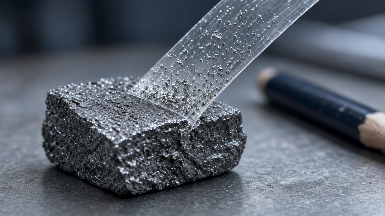
Andre Geim and Konstantin Novoselov, both at the University of Manchester, took a low-tech route. They pressed adhesive tape onto graphite and peeled it away. According to the Nobel summary, the first flakes were many layers thick, but repeating the tape trick ten to twenty times made them thinner and thinner.
The harder problem was finding a one-atom flake among the thicker scraps. Their second idea solved it. They laid the flakes on a wafer of oxidized silicon, the standard material of the chip industry. Under an ordinary microscope, the layer of silicon dioxide made the flakes show rainbow colors, like oil on water, and the color revealed how many layers each flake had. The thickness of that oxide layer was crucial to making graphene visible at all.
Their paper in Science on October 22, 2004 described graphitic films “a few atoms thick” that were “stable under ambient conditions, metallic, and of remarkably high quality.” Graphene had always existed, as the Nobel summary puts it. The trick was being able to spot it. In 2010, Geim and Novoselov shared the Nobel Prize in Physics “for groundbreaking experiments regarding the two-dimensional material graphene.”

Illustration: an artist’s take on a sheet so thin it shows rainbow colors, as graphene flakes do on oxidized silicon.
Why one layer of carbon behaves so strangely
Graphene’s structure is simple. Each basic unit is a ring of six carbon atoms, and the rings tile a plane like chicken wire. The Nobel summary credits that near-perfect ordering to the strong bonds between carbon atoms. Those bonds are also flexible enough to let the sheet stretch by up to 20% of its original size. Its properties, though, are anything but simple.
Its electrons act as if they have no mass
Graphene isn’t a metal, an insulator or a true semiconductor. Writing in Science in 2024, Mark Peplow describes it as a semimetal with zero band gap, “so the tiniest of nudges makes it conduct electricity.” The 2004 paper reported that applying a voltage could load the films with either electrons or their positive counterparts, holes, which flowed with room-temperature mobilities of about 10,000 cm²/V·s.
The deeper strangeness is in how those electrons move. The Nobel summary explains that electrons in graphene behave as if they have no mass, like photons. They travel at a constant speed of about one million meters per second. That lets physicists test quantum effects on a lab bench that would otherwise need a particle accelerator.
The strongest material ever measured
In 2008, a Columbia University team draped graphene flakes over tiny holes and pressed down with the tip of an atomic force microscope until the sheet broke. They reported a breaking strength of 42 newtons per meter and a Young’s modulus of 1.0 terapascal. In bulk terms, that is an intrinsic strength of 130 gigapascals, and the authors wrote that the experiments “establish graphene as the strongest material ever measured” (Lee et al., Science, 2008).
That 130-gigapascal figure is the source of the popular line that graphene is “200 times stronger than steel.” There’s a catch, though. Team leader James Hone told Science that the number came from imagining billions of perfect sheets stacked into a block, which would be impossible to build. “In any bulk material, the actual practical breaking strength is much lower than the intrinsic strength,” he said. The measurement describes a flawless sheet, not a beam you could buy.
Transparent, yet it stops helium
A single layer absorbs about 2.3% of white light, a value set by a fundamental constant of physics. That makes graphene nearly transparent yet still visible (Nair et al., Science, 2008). The Nobel summary adds that graphene conducts electricity as well as copper and heat better than any other known material. It is also so dense that not even helium atoms can pass through it.
From sticky tape to products: the hype problem
Taped flakes are tiny, measured in square micrometers, which is perfect for physics and useless for a factory. A route to scale came in 2009. A team in Texas showed that graphene grows as mostly single-layer sheets on copper foil from methane by chemical vapor deposition, or CVD, at sizes of about a square centimeter (Li et al., Science, 2009).
Then came the promises: rollable TVs, space elevators, chips without silicon. “Expectations were very, very high,” Geim told Science in 2024. “The companies I was involved in were mostly based on hype.” Peplow’s report lists the problems:
- CVD graphene turned out to be a patchwork of crystals, and the seams between them usually degrade its properties.
- Moving the sheet off the copper and into a device could tear it, wrinkle it or contaminate it.
- Most touchscreens still use indium tin oxide.
The word “graphene” also got stretched. Many products contain graphene oxide or graphene nanoplatelets, which are multilayer or chemically modified forms with very different properties. As layers stack up, Peplow writes, graphene’s “superpowers decline,” and some properties of 10-layer stacks become indistinguishable from graphite’s. In 2017, the International Organization for Standardization ruled that “graphene” should mean a single layer, with “few-layer graphene” covering three to ten layers.
Those humbler forms are where most of the money is now. A 2024 analysis in Nature Reviews Physics counted more than 150,000 graphene-related patents. It found that, despite early promises for chips and photonics, the biggest applications so far have been energy storage and polymers. According to Science, Huawei began using graphene oxide to draw heat from smartphone circuits in 2019, and one supplier estimates its graphene oxide is now inside millions of electronic devices. The engineering director of the University of Manchester’s Graphene Engineering Innovation Centre told the magazine that a Ford engine foam part containing nanoplatelets has gone into more than 5 million U.S. vehicles. The market research firm IDTechEx puts the market for all types of graphene at about $150 million a year.
Graphene isn’t the only material that conducts in surprising ways. Odinity’s lab report on the synthesis and properties of polyaniline, a plastic that conducts electricity, shows another route to the same goal. The quantum dot nanocrystals experiment explores another nanomaterial whose behavior is ruled by quantum effects.
What’s settled and what’s still open
Settled:
- Single-layer graphene exists and is stable at room temperature.
- Its electrons behave as if they have no mass.
- A flawless sheet has the highest intrinsic strength ever measured.
- It absorbs about 2.3% of white light.
The Nobel committee’s 2010 popular summary describes graphene as stable at room temperature, the strongest material known, almost completely transparent and home to electrons that behave as if they have no mass.
Still open:
- Electronics. An editorial in Nature Electronics marking the 20th anniversary called it “still an open question” how graphene and other 2D materials can break into chipmaking and justify the cost of switching.
- Reproducibility. Peter Bøggild of the Technical University of Denmark told Science that surprisingly few published procedures for handling and transferring CVD graphene can be reliably repeated.
- Twisted layers. Researchers have found that twisting one layer of a two-layer stack by 1.1° turns it into a superconductor. Whether such stacks lead to real devices is, in the words of one Manchester physicist, going to “need more time.”
Geim himself told Science he would “spread my bets” across many 2D materials rather than graphene alone. So graphene is real, and it is as strange as the physics promised, but the material in most products isn’t quite what was peeled off with tape in 2004.